A Place to Start
Making things
Well, it’s been a while since I’ve started this project !
In July of 2024, I realized that for a while I didn’t made something that require commitment, in a sense that my actual work (software developpement and cloud architecture) don’t require me to make technical decisions that cannot be quickly adapated/changed.
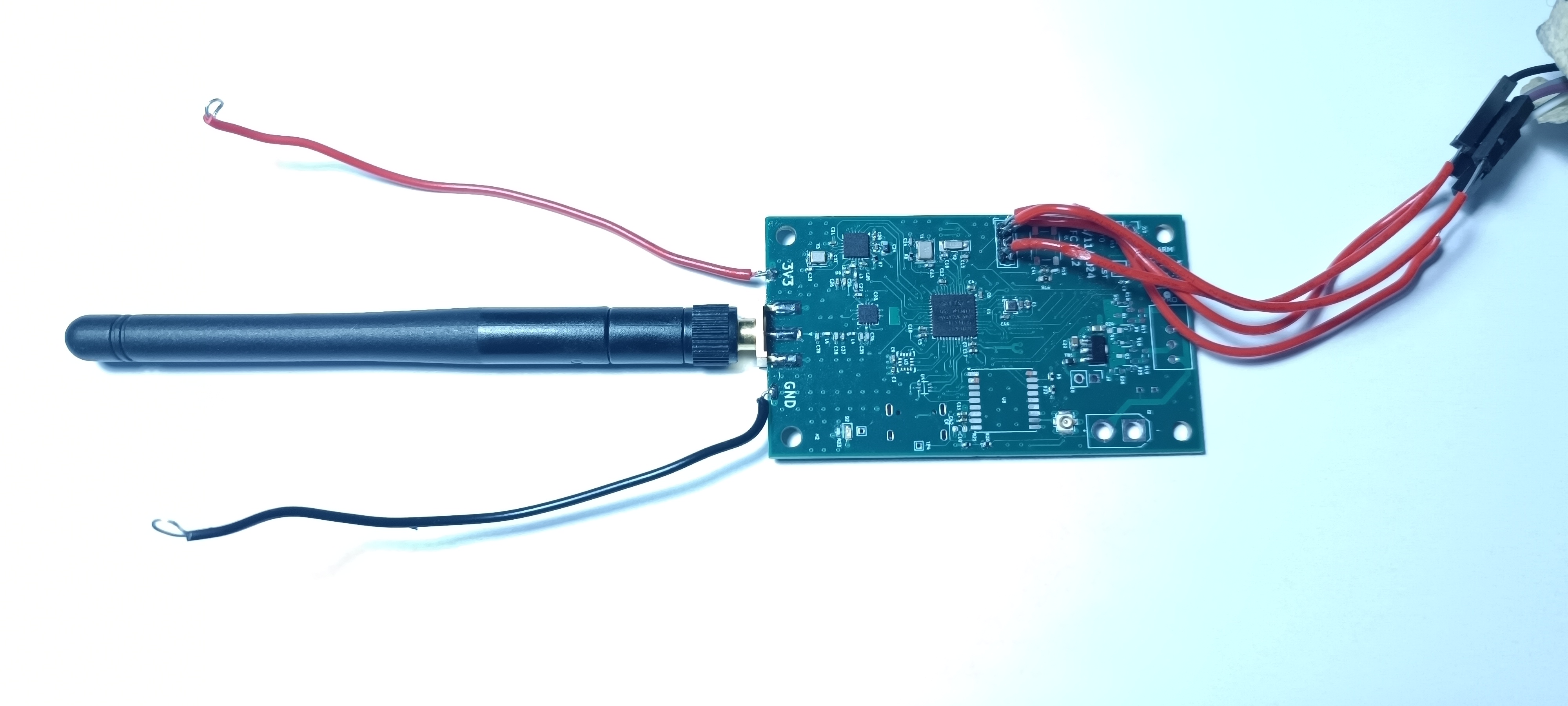
So I decided to build my own flight computer for model rocket (yes it’s a thing) !
I will detail the developpement process and what are my progress so far in future articles, but for now I really want to share what challenged I’ve faced prototyping and designing a custom PCB, as someone who’s main job is to build softwares.
What’s hard about making hardware design
Let’s pretend that I want to implement a data format used to transfer data between two APIs (let’s say a JSON).
Halfway through the developpement process I could realize that some modifications are needed to the content (some fields must be renamed for example).
To do so I can simply modify the data structure, make some adjustments in the code and that’s should do.
The only real cost here is the time consumed, but the modification can be implemented immedialty, and more importantly, it can be tested and validated directly, without any additional cost involved.
And, in the eventuality of more rework later, it is stil possible !
In other words, it shape the brain to think and develop solution to problem in a iterative manner, because it’s possible to do so. If the first try wasn’t the right one, you can always make a new attemps very quickly.
So, when you transition from building software to hardware (like designing a custom PCB), you have a new set of constraints added to your developpement workflow.
Everytime you want to add a new feature or change something already existing and in order to test it, it is required to get theses PCB fabricated, shipped, and then tested.
For someone who’s sollely used to work in a controlled environment (cloud mainly), with the possibility to rollback when bad things happens, it’s is absolutely intimadating to step into this unforgiving world that is PCB design
Building discipline
After spending some time learning how to use software like Kicad, and rapidly growing a good understanding of how to translate my ideas into schematics (which I already new but for simple circuits), I wanted to regain trust in my ability to build electronics circuits.
I started building a prototype using perfboards and dev-boards for sensors and MCU. It allow the brain to progressively get used to take risk while making decisons about placements, soldering, while being free to unsolder everything if needed (which I did mainy times).
Doing so while having that safety net of being able to reconsider my technical decisions as I progressed into the developpement cycle, let me go being my fear of failing, and eventually being confortable designing a custom PCB.
In the end reducing errors while implementing systems that cannot be tested beforehand can be acheived by first making a good and comprenhensible design, and be very rigourous while reading datasheets and making schematics.
I’ts easier said than done though. Sometime datasheet are confusing, sometimes sensors does not have prebuilt drivers, adding more work and possible issues once the PCB is fabricated and assembled. All of this contribute to the difficulty of this field (PCB design).
Conclusion
For me, going outside your confort zone (which is what this article is all about) is really what make you become better, not only in the field you want to discover/learn about, be also as a person.
It shape your brain to accept disconfort, and make you mesure your own ignorance to better overcome the challenge.
Step by step we’ll make it there eventually, but it requires time patience, and in case of designing custom PCB, a bit of money ^^.
V.